


What is EUV? The ultimate guide
Learn about EUV lithography's role in microchip production & understand Moore’s Law's impact on computing speed & capability.
Extreme ultraviolet (EUV) light technology is revolutionizing the semiconductor industry. Lithography, the technique employed to print detailed patterns onto semiconductor materials, has continuously evolved by utilizing progressively shorter wavelengths since the dawn of the semiconductor era. EUV lithography represents the pinnacle of this advancement with the shortest wavelength yet.
After decades of development, ASML, a Dutch semiconductor company, became the first to sell EUV lithography machines in batches that are ready for production.
What Is EUV Lithography?
EUV light, or extreme ultraviolet light, is utilized in microchip lithography. This process involves coating a microchip wafer with a photosensitive material and then exposing it to light, printing a pattern onto the wafer that is essential for subsequent microchip design steps.
The evolution of computers is intertwined with the semiconductor industry's quest for miniaturization. From the 1950s to the mid-1980s, photolithography used UV light and photomasks to project circuit patterns onto silicon wafers. However, by the 1960s, Moore's Law—which predicted that the number of transistors on a microchip would double every two years—began to face the physical limitations of this process, threatening the rapid increases in computing power and reductions in technology costs.
From the 1980s to the 2000s, deep ultraviolet (DUV) lithography, utilizing shorter wavelengths of 153 to 248 nanometers, enabled further miniaturization by allowing smaller imprints on silicon wafers. Approaching the new millennium, global researchers and competing firms sought breakthroughs to make EUV lithography and its even shorter wavelengths viable.
ASML, a Dutch semiconductor company, completed a prototype EUV lithography system in 2003, but it took another decade to create a production-ready system. Since then, ASML has consistently delivered advanced EUV lithography systems every few years, achieving wavelengths as short as 13.5 nanometers. This technology allows for extremely precise microchip designs and the densest placement of transistors, resulting in significantly faster computer speeds.
How EUV lithography operates
ASML's EUV lithography systems utilize light with wavelengths around 13.5 nanometers, significantly shorter than those used in previous DUV lithography generations. This enables the printing of finer patterns on semiconductor wafers. Advanced microchips with nodes as small as 7, 5, and 3 nanometers are produced by repeatedly exposing semiconductor wafers to the EUV lithography system.
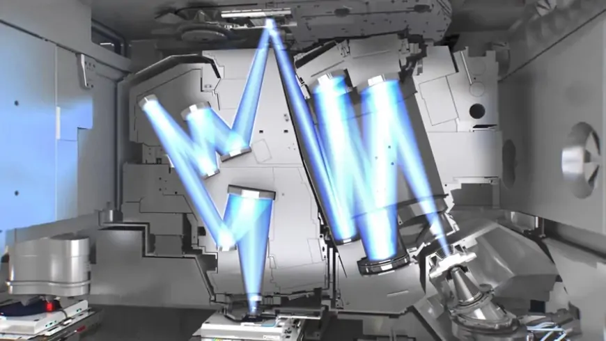
While these processes cannot be replicated in a garage workshop, understanding them is crucial for recognizing opportunities for technological advancement and strategic investment. Initially, a high-intensity laser targets a material, typically tin, to create plasma—a state of charged electrons and protons in motion. This plasma emits EUV light at approximately 13.5 nanometers. The emitted light is collected and directed through a sequence of mirrors and optics onto a mask or reticle containing a circuit pattern. This process is akin to using a stencil to apply a pattern on a surface. The semiconductor wafer, coated with a light-sensitive material called photoresist, undergoes a chemical transformation in exposed areas upon exposure to EUV light. Subsequently, new materials are deposited into these etched areas to form various microchip components. This iterative process, involving up to 100 cycles with different masks, enables the creation of complex, multilayered circuits on a single wafer. Following these steps, the wafer undergoes additional processes to eliminate impurities before being cut into individual chips and packaged for integration into electronic devices.
Comparison of EUV and DUV lithography
While EUV lithography systems have garnered attention in the semiconductor industry due to their potential technological advancements and significant costs, DUV lithography remains more widely adopted. DUV lithography, operating at wavelengths starting from 153 nanometers, is currently employed in manufacturing facilities with established workflows and trained staff.
EUV lithography, utilizing extremely short wavelengths around 13.5 nanometers, allows for finer etching of smaller features on chips. In contrast, DUV lithography can handle designs with sizes as small as 5 nanometers or less, albeit with reduced resolution quality. Despite the technological advantages of EUV lithography, its adoption is hindered by high startup costs and ongoing expenses compared to DUV lithography. For instance, Intel's 2023 installation of EUV lithography systems cost $150 million each, highlighting its substantial financial investment.
DUV lithography's established presence and lower operational complexity make it preferable for applications where the enhanced capabilities of EUV lithography are unnecessary. Moreover, DUV lithography's efficiency in producing more chips per unit time contributes to its continued relevance amid global semiconductor demand. While EUV lithography is expected to grow in significance, DUV lithography remains crucial for manufacturing chips used in everyday electronics like phones, computers, cars, and robots. Thus, DUV lithography is anticipated to maintain its popularity for years, evolving alongside advancements in semiconductor technology.
Pros and cons of EUV lithography
Pros of EUV Lithography
EUV lithography offers significant advantages that could pave the way for advancements in microchip manufacturing. These are two key reasons why semiconductor companies, such as Intel, are heavily investing in this technology:
- EUV light enables the creation of more intricate and precise patterns on silicon wafers, facilitating higher transistor densities on microchips.
- EUV lithography reduces the number of pattern layers (masks) needed to manufacture a circuit, streamlining the production process.
Cons of EUV lithography
While EUV lithography offers substantial benefits, it also comes with certain challenges to consider:
- EUV lithography systems are significantly more expensive than other microchip lithography systems, posing a barrier to adoption for some semiconductor manufacturers.
- ASML is currently the sole manufacturer of EUV lithography systems, potentially creating a bottleneck for companies seeking to adopt this technology or requiring support for their equipment.
Future alternatives to EUV lithography
As technology advances and the demand for microchips with denser transistor arrays grows, ongoing research explores alternatives to or improvements upon EUV lithography. Potential successors include multi-e-beam, X-ray lithography, nanoimprint lithography, and quantum lithography, each aiming to surpass or enhance current capabilities in microchip production.
When is EUV light used?
Extreme ultraviolet (EUV) light is utilized in the manufacturing of microchips through EUV lithography, which prints intricate patterns onto silicon wafers.
What is Moore’s law?
Moore’s Law posits that the number of transistors on a microchip doubles approximately every two years, leading to exponential increases in computing speed and capability. Named after Gordon E. Moore, co-founder of Intel, the law held true for decades, though some anticipate its potential limitations in the 2020s.


